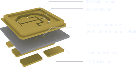
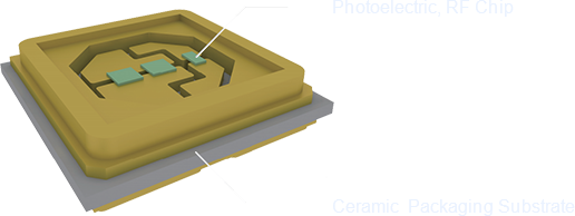
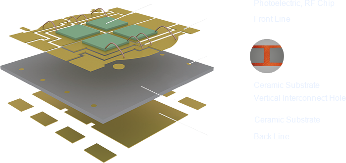
Thin Film Circuit Ceramic Packaging Substrate

Thin-film circuit ceramic packaging substrate is a technology combining the film metallization and electroplating process of thin film:Namely according to the application requirements, 2D metal circuits are fabricated on high thermal conductive ceramic substrates by means of film metallization and image transfer. Then TCV(Through Ceramic Via) technology is used to form a vertical interconnection between double-sided wiring, and finally stacking technology is used to obtain an integrated 3D metal frame which is tightly bound to the ceramic substrate.

PRODUCT DETAILS

产品细节图

FEATURES

产品特点

PRODUCT CENTER

产品中心
Ceramic Package Substrate
For 5G Radio Frequency
Thin-film circuit ceramic packaging substrates are widely used in 5G RF front-end discrete devices and module packaging due to their high reliability, high thermal conductivity, high circuit resolution, high circuit flatness, and excellent noise reduction and anti-interference capabilities.
Ceramic Package Substrate
For 5G Optoelectronics
Thin-film circuit ceramic packaging substrates are widely used in 5G optoelectronic devices such as LED lighting, UV LED, car lights, flashlights, face recognition, and Lidar due to their high reliability, high thermal conductivity, high circuit resolution, high circuit flatness.