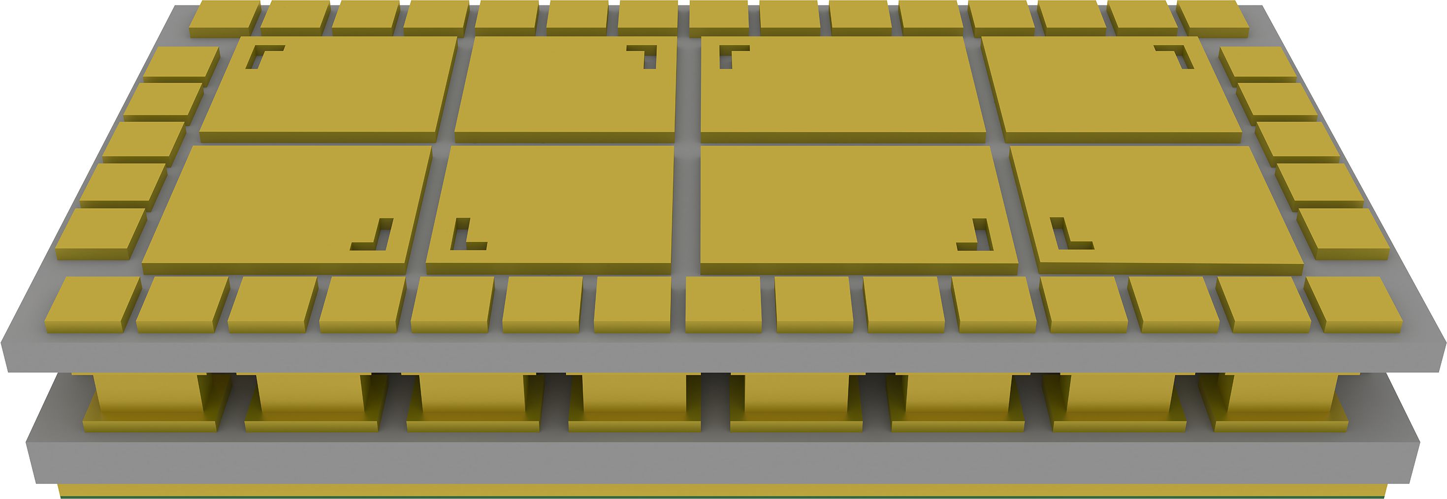
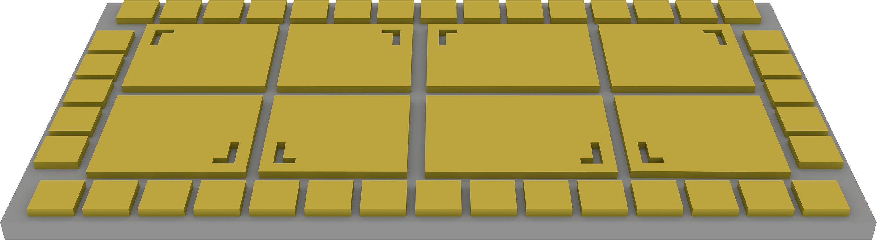
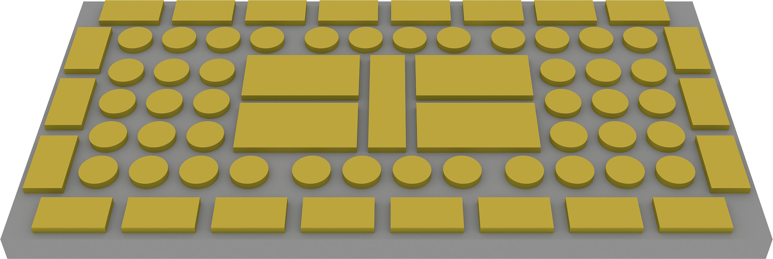
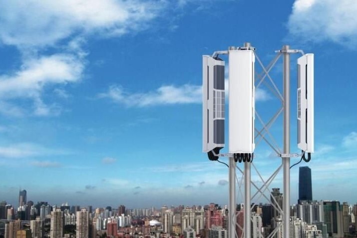
Thin-film circuit ceramic packaging substrates are widely used in 5G RF front-end discrete devices and module packaging due to their high reliability, high thermal conductivity, high circuit resolution, high circuit flatness, and excellent noise reduction and anti-interference capabilities.
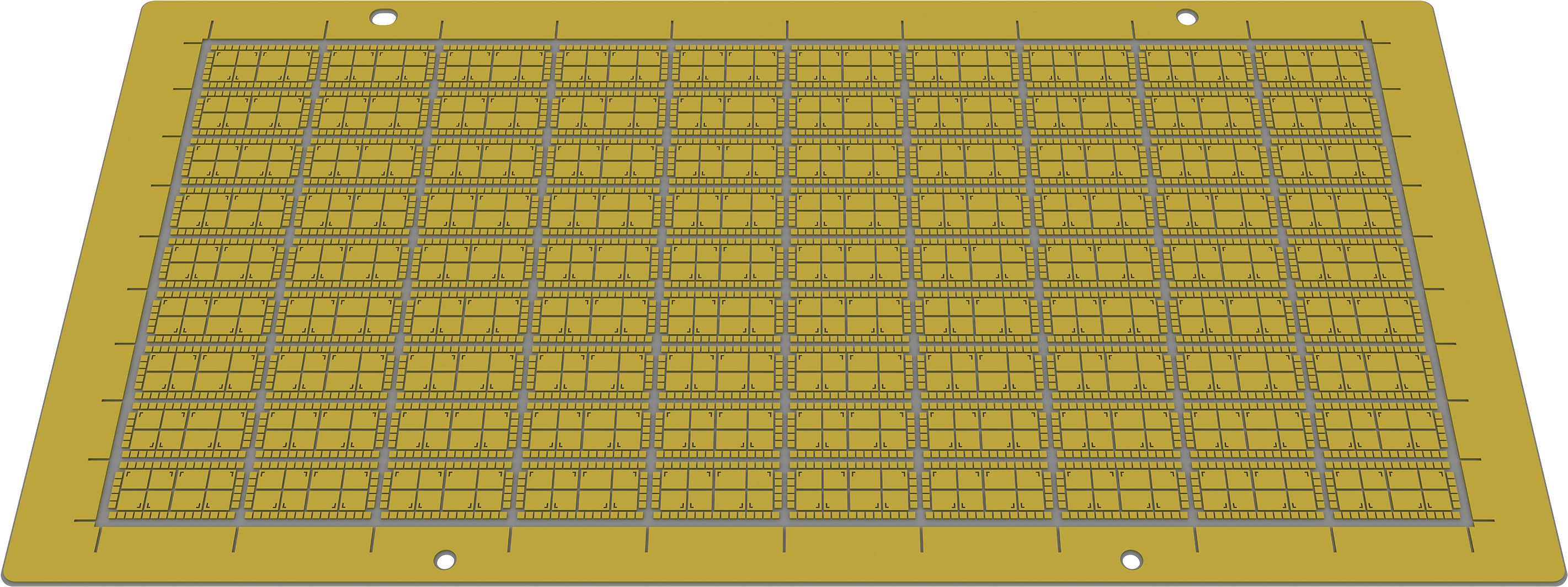
Model:
9550Material:
Alumina/aluminum nitrideSubstrate Thickness:
0.69±0.15 mmNumber Of Typeset:
90 pcs/sheetSheet Size:
109.2×54.5 mmSingle Size:
9.45×4.76 mmMinimum Line Width:
0.13 mmGap Size:
0.15 mmMinimum Aperture:
0.07 mmCopper Thickness:
65±15 μmDam Thickness:
Step Height:
Boss Copper Thickness:
Metal Column High:
400±50 μm