Rich experience, mature technology; Perfect solution to the conductive hole cavity problem.
Perfect R & D, process, production and quality system.
Design the close arrangement structure to reduce the cost.
Sample: 10-15 days delivery.
Order: Short lead time and flexible delivery.
The transportation and logistics are very convenient.
Customer first, Smooth communication,attentive service, quick response.
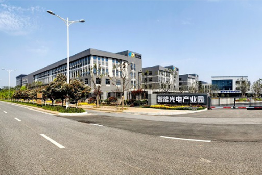
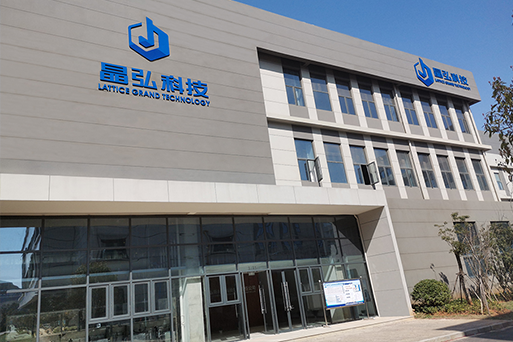
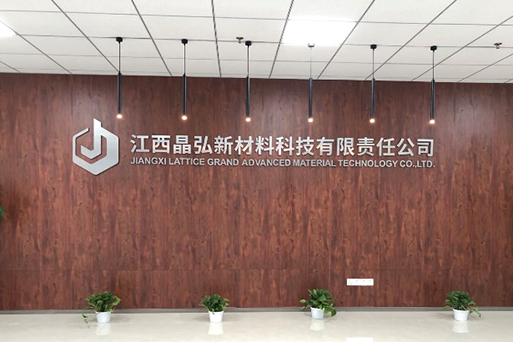
Jiangxi lattice grand advanced material technology co., ltd. was founded in July 2020. The company is located in Intelligent Photoelectric Industrial Park, Third Xianghe Road,Linkong Economic Zone, Nanchang, Jiangxi Province. It covers an area of about 10,000 square meters and has more than 100 employees, including more than 40 bachelor's degree holders. It is a thin film circuit ceramic substrate manufacturer with research and development, manufacturing and sales. The company has a self-trained professional technology research and development team, advanced production management system, systematic decision-making process, committed to providing fast, professional and cost-effective products and perfect solutions for global customers.
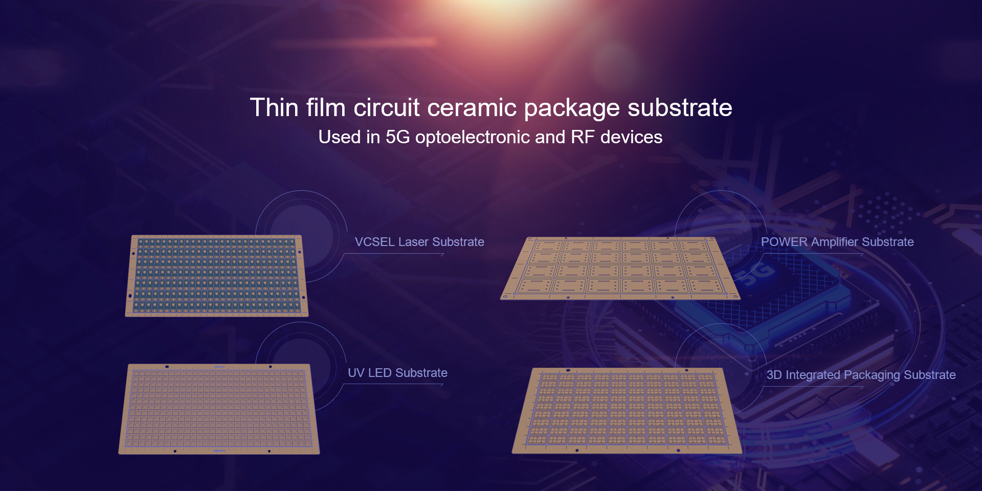
The company's main product is a based film circuit packaging process of high thermal ceramic packaging substrate. Namely, film metallization, image transfer and TCV(Through Ceramic Via) technology are adopted in ceramic substrates with high heat conduction the formation of high density double sided wiring and vertical interconnection, finally, the stacking technique is used to obtain an integrated 3D metal frame which is tightly bound to the ceramic matrix. The company's products conform to the semiconductor device miniaturization, integration, high heat dissipation, airtightness, self-shielding and other packaging requirements. It is the ideal packaging substrate for semiconductor lighting, power electronics, optoelectronics, microwave radio frequency and other fields.